With the simulation software, our individual virtual “lab tools”, you can conduct various virtual experiments on digital twins of OLED materials, layers and devices. In the following we want to highlight some applications:
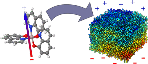
- GSP: Analyze giant surface potential in a thin film of Alq3 and CBP (link)
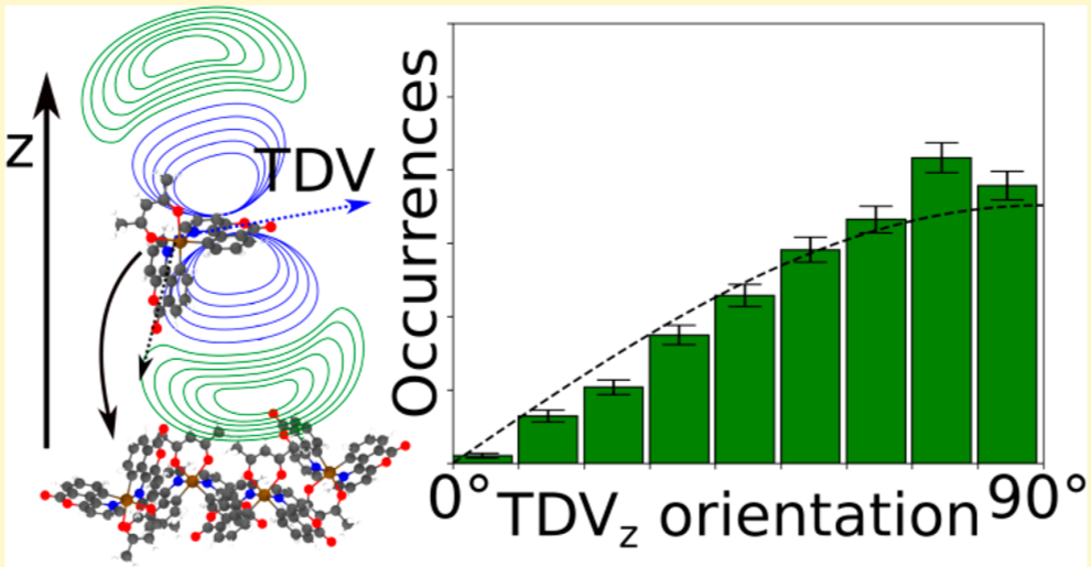
- Improving outcoupling: Analysis of emitter orientation in organic films
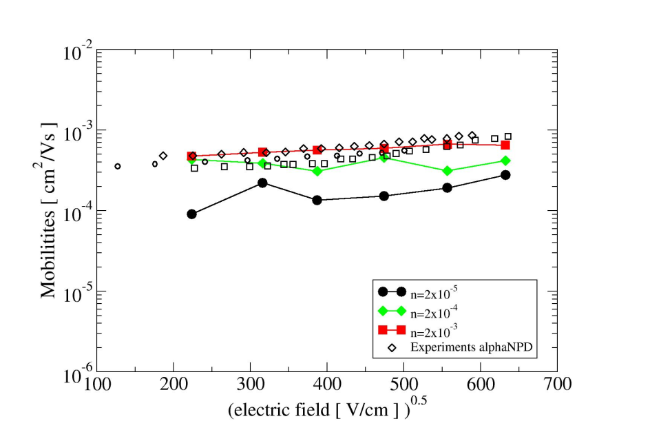
- Time-of-flight (TOF) “measurement”: Computation of charge mobility of pristine and mixed layers
These use-cases are also included as pre-defined simulation workflows in the trial version of the virtual lab (available for download here), and you can find a more detailed description below and on the respective subpages.
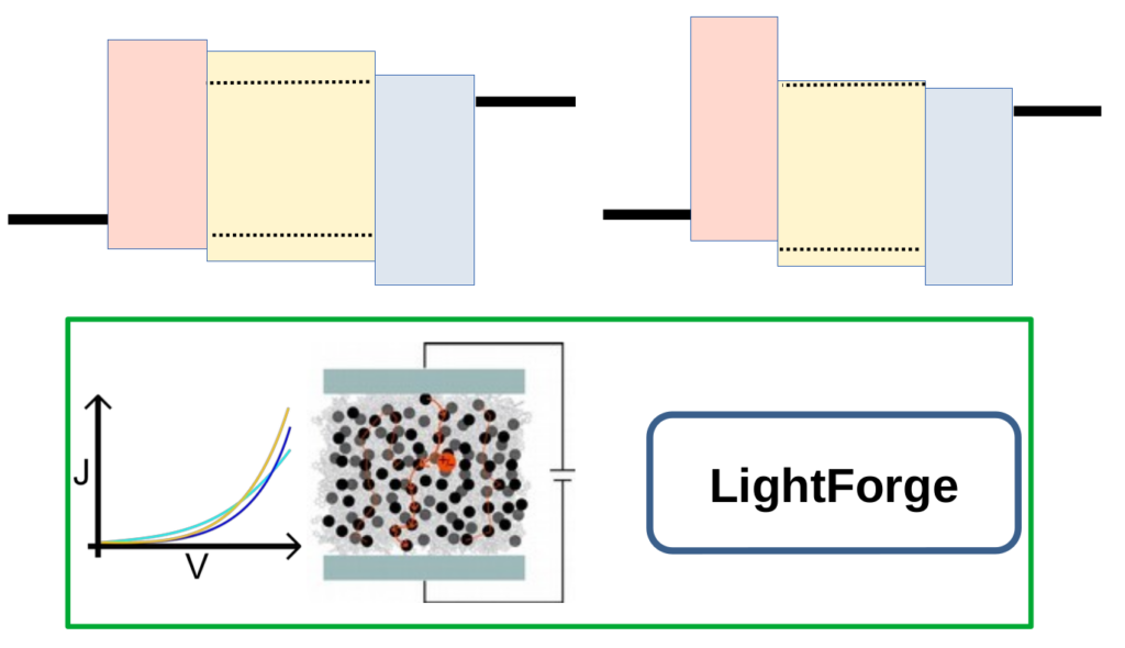
These four virtual experiments are just a fraction of potential applications of the virtual lab and the multiscale simulation approach can be applied to address further challenges in organic electronics, such as the charge carrier balance and exciton dynamics in multilayer OLED stacks (e.g. for alpha-NPD:Ir(piq)3, see here(link)) or virtual photoluminescence quenching (PLQ) experiments to analyze loss processes in emission layers. If you are interested in a particular application, especially if not listed above, contact us at virtuallab@nanomatch.com
GSP: Anisotropic orientation of molecules during the deposition process can lead to built-in potentials, so called giant surface potentials, GSP, in organic thin films. Here we show you how to compute GSP in thin films of CBP and Alq3 using the simulation modules Parametrizer, DihedralParametrizer, Deposit and the GSP Analysis tool. Read the full description.
Figure from: P. Friederich et al. ACS Appl. Mater. Interfaces 2018, 10, 1881−1887
The orientation of emitter molecules in organic layers depends on the interaction with their host materials. Here we present a systematic study of the impact of functional side groups of emitter molecules on the alignment of their transition dipoles in a CBP host, and illustrate how virtual experiments can aid the design of emitter molecules. Read the full description.
Figure from: P. Friederich et al. Chem. Mater. 2017, 29, 9528-9535
TOF “measurement”: In this application we explain how to compute charge carrier mobility of different materials from first principles using the seamless multiscale workflow: we generate a digital twin of the organic layer using Deposit, then run virtual spectroscopy experiments with QuantumPatch and finally conduct virtual TOF measurements with LightForge. Read the full description.
Microscopic simulations of charge carrier and exciton dynamics can serve as virtual microscope. Detailed analysis of excitonic processes for a specific setup can aid to identify and understand microscopic bottlenecks and help to develop design rules for optimized OLEDs. Here we illustrate how to set up a three-layer model phOLED and a TTF OLED in LightForge and how to analyze exciton dynamics in both systems. Read the full description.


