|
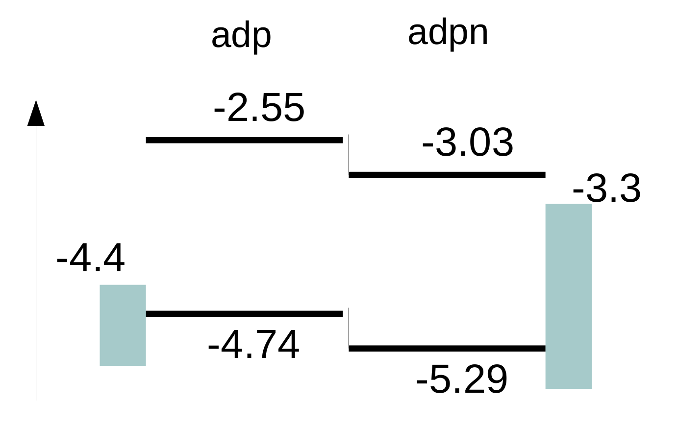
In this use case we demonstrate how the full Nanomatch software stack is applied to compute essential properties of an OLED stack: J-V characteristics, charge distribution along the device and quantum efficiency. In order to highlight the methodology, we restricted ourselves to the simplest model: a bilayer OLED. While this setup is a rather “bad” OLED in terms of quantum efficiency, it illustrates the application of all modules in the OLED workflow, and extension to arbitrarily complex multilayer stacks is straight forward. The minimal working example in this use case is a bilayer OLED stack consisting of the molecules ADP and ADP with two carbons substituted by Nitrogen (thereby lowering the orbital energy levels) ADP/N. A schematic setup is illustrated in the Figure to the left. In order to compute the device characteristings starting from first principles, we follow the standard OLED workflow used in many applications. |
 |
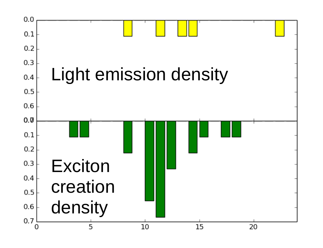
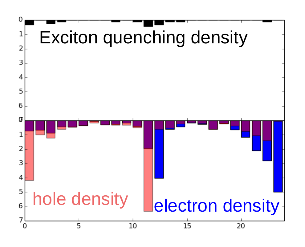
| For this setup, we computed orbital energy levels throughout the device, IQE and I-V, as well as the distribution of charge carriers and excitons throughout the device and light emission density. From these results we can conclude the following: First, high charge carrier density (of both types) leads to strong exciton quenching and thereby reduces IQE. OLED efficiency can therefore be improved by balancing charge carrier distribution and spatially separate charge accumulation and exciton creation, e. g. by including guest-host emission layers. Second, there is non-vanishing density of holes and electrons at the electrode opposite to their injection and charge carriers are lost by traveling to the opposite electrode. This can be overcome by including electron- or hole-blocking layers next to the emission layer. |  |
| Read the full use case for further information. |  |